The thought of an interview can be nerve-wracking, but the right preparation can make all the difference. Explore this comprehensive guide to Mask Design and Development interview questions and gain the confidence you need to showcase your abilities and secure the role.
Questions Asked in Mask Design and Development Interview
Q 1. Explain the difference between optical and electron-beam lithography in mask making.
Optical lithography and electron-beam lithography (EBL) are both used in mask making, but they differ significantly in their approach to pattern transfer. Optical lithography uses ultraviolet (UV) light projected through a mask to create patterns on a photosensitive material (resist) coated on a wafer. Think of it like a shadow puppet show—the mask blocks and transmits light to create the desired pattern. The resolution is limited by the wavelength of the light used and the optics’ quality.
Electron-beam lithography, on the other hand, uses a finely focused beam of electrons to directly write patterns onto the resist. It’s like using a super-precise pen to draw the pattern directly on the wafer. This offers much higher resolution than optical lithography as the electron beam’s wavelength is much shorter. However, EBL is significantly slower and more expensive than optical lithography, making it more suitable for smaller-scale, high-resolution applications such as creating photomasks themselves.
In essence, optical lithography is like a mass production method, while EBL is a more precise but slower, bespoke process. The choice between the two depends on the required resolution, throughput, and cost considerations of the project. For example, mass production of integrated circuits would use optical lithography, whereas creating a high-resolution mask for specialized applications might favor EBL.
Q 2. Describe the critical dimensions (CD) in mask design and their impact on device performance.
Critical dimensions (CDs) in mask design refer to the physical dimensions of the features on the mask, such as the width of lines and spaces, the size of contacts, and the spacing between features. These dimensions are crucial because they directly influence the dimensions of the features transferred onto the wafer during the lithographic process and ultimately impact the performance of the final device.
For instance, in a transistor, the gate length, which is a CD, directly impacts its switching speed and power consumption. A smaller gate length usually translates to faster switching but can also lead to increased leakage current. Similarly, the spacing between interconnect lines (another CD) affects their capacitance and resistance, influencing signal delay and power consumption. Variations in CDs—called CD variations—can lead to device mismatch and performance degradation across the wafer, thus stringent control of CDs during mask design and manufacturing is critical. It is a key contributor to process control and yield in semiconductor manufacturing.
In practice, maintaining accurate CDs within very tight tolerances (often nanometers) is essential for reliable device operation. Advanced techniques like Optical Proximity Correction (OPC) are employed to compensate for the effects of diffraction and other factors that can cause CD variations during the lithographic process.
Q 3. What are the key challenges in designing masks for EUV lithography?
EUV lithography, using extreme ultraviolet light (wavelength ~13.5nm), offers the highest resolution currently available for semiconductor manufacturing, enabling the creation of incredibly small features. However, designing masks for EUV presents unique challenges.
- Mask Blank Defects: EUV light is highly sensitive to defects on the mask blank. Even tiny defects can significantly affect the patterned image on the wafer, leading to yield losses. Therefore, extremely high quality mask blanks are required.
- High-Resolution Pattern Design: The extremely small feature sizes in EUV require highly sophisticated design techniques and advanced simulation tools. Managing resist effects and achieving sufficient process window for manufacturing are particularly challenging.
- Mask-Induced Aberrations: The mask itself can introduce distortions into the projected image, requiring advanced correction techniques to mitigate these aberrations. These corrections are more complex than in previous lithographic techniques.
- High Cost and Complexity: EUV lithography equipment and processes are extremely expensive and complex, requiring highly skilled personnel to operate and maintain them. The cost of mask production itself is considerably higher than for previous generations of lithography.
Overcoming these challenges requires advanced materials, sophisticated design methodologies, highly precise manufacturing techniques, and robust metrology methods to ensure accurate and defect-free EUV masks.
Q 4. How do you ensure the accuracy and precision of mask designs?
Ensuring the accuracy and precision of mask designs is paramount. A multi-faceted approach is used, starting with rigorous design rules that define the minimum and maximum feature sizes and spacing. These rules are based on the capabilities of the lithographic process and are crucial for manufacturing feasibility. Then, various verification techniques are used to catch errors early in the design cycle.
- Design Rule Checking (DRC): DRC software automatically verifies that the design meets all specified design rules. Any violations are flagged and require correction.
- Optical Proximity Correction (OPC): OPC models the effects of diffraction and other optical phenomena and adjusts the mask pattern to compensate for these effects, leading to more accurate feature placement and dimensions on the wafer.
- Process Simulation: Process simulation models the entire lithographic process, including resist behavior and development, to predict the final pattern on the wafer. This allows for early detection of potential problems.
- Verification through Layout vs. Geometry comparisons: Verifying that the final layout after OPC matches the design intent. This might involve comparing the generated geometry against the initial design specifications to confirm the efficacy of OPC and rule checking.
- Mask Metrology: After mask fabrication, rigorous metrology measurements are performed to verify the actual dimensions and placement of features on the mask, comparing them to the design specifications.
By employing these techniques, we can minimize errors and ensure the mask accurately reflects the intended design. A combination of automated checks and manual review ensures highest possible accuracy.
Q 5. What software and tools are you familiar with for mask design and verification?
My expertise spans several software and tools used in mask design and verification. I’m proficient in industry-standard EDA (Electronic Design Automation) tools, including:
- Calibre (Mentor Graphics): A comprehensive suite of tools for layout verification, including DRC, LVS (Layout Versus Schematic) verification, and OPC.
- Synopsys IC Compiler and Innovus: Used for physical design and verification.
- KLayout: An open-source tool useful for mask design visualization, editing and analysis.
- Various OPC software packages from vendors like Synopsys and ASML: Essential for correcting optical proximity effects and ensuring accurate pattern transfer.
- Process simulation software like Solid-e: Allows for accurate prediction of the final pattern on the wafer after lithography.
I’m also familiar with scripting languages like Python and TCL, commonly used for automating tasks and customizing workflows within these EDA tools. My experience encompasses the entire workflow, from initial schematic creation to final mask data preparation for manufacturing.
Q 6. Explain the concept of Optical Proximity Correction (OPC) and its role in mask design.
Optical Proximity Correction (OPC) is a crucial technique in mask design that compensates for the limitations of the optical lithography process. During lithography, light diffracts as it passes through the mask and the resist, leading to deviations from the intended pattern on the wafer. These deviations can result in inaccurate feature sizes and shapes, impacting device performance and yield.
OPC involves modifying the mask pattern itself to counteract these diffraction effects. Essentially, the features on the mask are deliberately altered to produce the desired final pattern on the wafer. This involves sophisticated algorithms that model the optical behavior of light during lithography. Different OPC models use various algorithms and parameters. For example, some models account for process variability, while others use a more detailed model of the light source and optics.
For example, a small feature might appear smaller than intended on the wafer due to diffraction. OPC would enlarge the feature on the mask to compensate for this effect. This ensures higher fidelity in the reproduced patterns on the chip.
OPC significantly improves the accuracy of the printed patterns, enabling the fabrication of smaller and denser integrated circuits. It is essential for achieving high yields and performance in advanced semiconductor manufacturing. Without OPC, the creation of modern chips with extremely small features would be impossible.
Q 7. How do you handle design rule checking (DRC) violations during mask design?
Design rule checking (DRC) violations indicate that the mask design doesn’t adhere to the predefined rules governing minimum feature sizes, spacing, and other critical parameters. Handling these violations requires a systematic approach:
- Identify the Violations: DRC software identifies the specific locations and types of violations in the design.
- Analyze the Root Cause: Understanding why the violation occurred is critical. Common causes include unintentional overlaps, insufficient spacing between features, or features that are too small. A thorough analysis often requires careful visual inspection and understanding of design intent.
- Implement Corrections: Depending on the severity and nature of the violation, corrections can range from simple adjustments to the layout to more extensive redesign efforts. Simple violations might only need a minor tweak in spacing, whereas more complex cases might require significant design changes.
- Re-run DRC: After implementing corrections, it’s crucial to re-run the DRC to ensure the violations have been resolved and no new ones have been introduced. This iterative process ensures that all violations are identified and corrected before proceeding to the next stages of the mask making process.
- Consider OPC interaction: It is important to consider the impact of OPC on the design rules. Sometimes minor design changes, to resolve a DRC violation, may impact the effectiveness of OPC, hence it is crucial to verify the combined impact of DRC fixing and OPC.
Effective DRC management is essential to guarantee manufacturing feasibility and yield. Neglecting DRC violations can lead to significant problems during manufacturing, impacting costs and timelines.
Q 8. Describe your experience with different mask materials and their properties.
Mask materials significantly impact the quality and performance of the final product. My experience encompasses a wide range, from traditional materials to advanced ones. For instance, I’ve extensively worked with:
- Quartz: Known for its excellent transparency at deep ultraviolet (DUV) wavelengths, making it ideal for high-resolution lithography. Its thermal stability is crucial for high-temperature processes. However, its cost can be a factor.
- Silicon: A substrate choice often used for its mechanical strength and ability to support various thin-film layers. Its suitability varies depending on the specific application and design requirements.
- Low-k dielectrics: These materials are incorporated in advanced masks to reduce capacitance, improving performance in high-speed circuits. The challenge lies in ensuring their compatibility with other mask layers and processing steps.
- Chrome: Often used as an absorber layer, its thickness and patterning accuracy are critical to defining the features on the final chip. I’ve experimented with different chrome formulations to optimize its reflectivity and etch characteristics.
Each material’s properties—refractive index, thermal expansion coefficient, etch rate, and stress—need careful consideration during the design phase to prevent defects and ensure optimal performance. For example, choosing a material with a high stress can lead to warping, rendering the mask unusable.
Q 9. How do you ensure the manufacturability of your mask designs?
Manufacturability is paramount. I employ a design-for-manufacturing (DFM) approach from the outset. This involves:
- Process Window Analysis: This involves simulating the etching, deposition, and other processes to assess the tolerances and robustness of the design. We ensure the design is robust enough to account for variations in the manufacturing process.
- Design Rule Checking (DRC): This is an essential step to verify the design against the fabrication rules provided by the foundry. Automated DRC tools are used to flag any potential violations, ensuring the mask is manufacturable.
- Layout Optimization: Techniques like layout compaction and pattern generation are used to optimize the mask layout, ensuring efficient use of space and minimizing defects. This often involves careful placement of critical features and consideration of process-induced distortions.
- Collaboration with Foundries: Close communication with the foundry is vital. Early involvement allows us to incorporate their feedback and constraints into the design, ultimately increasing the likelihood of a successful fabrication run.
For instance, I once had to redesign a section of a mask due to a tight clearance that violated the foundry’s minimum feature size rules. By strategically modifying the layout and working with the foundry engineers, we successfully overcame this issue.
Q 10. What are the different types of mask defects and how are they detected?
Mask defects can significantly impact yield and product quality. They can broadly be categorized as:
- Geometric Defects: These relate to the dimensions and shapes of the features, such as line width variations, bridging, and pinholes. These often stem from issues in the mask fabrication process.
- Photo-mask Defects: These can be caused by particle contamination, film defects (scratches, pinholes), or variations in the coating processes.
- Optical Defects: These affect the optical performance of the mask, including optical proximity correction (OPC) errors and distortions.
Detection methods involve a multi-pronged approach:
- Optical Inspection: Using high-resolution microscopes and automated inspection tools to detect surface defects.
- Scanning Electron Microscopy (SEM): Provides higher resolution for detecting smaller defects and critical dimension (CD) measurements.
- Defect Review and Analysis: A thorough review of inspection results is vital to classify and analyze defects, trace their root causes, and implement corrective actions.
For instance, we once detected a recurring pattern of pinholes in a particular region of a mask. Through detailed analysis, we traced this to an issue in the chrome deposition process, allowing the foundry to adjust its parameters and prevent future occurrences.
Q 11. Explain your experience with mask data preparation and management.
Mask data management is crucial for efficient design and collaboration. My experience involves:
- Data Formats: Proficiency in various data formats such as GDSII, OASIS, and CIF, understanding their structure and limitations is crucial for smooth data exchange.
- Data Integrity: Implementing robust version control and backup systems to maintain data integrity and prevent data loss. This is particularly important in large-scale projects.
- Data Management Software: Experience with Electronic Design Automation (EDA) software and data management tools allows for efficient data handling, design rule checking (DRC), and layout verification.
- Data Exchange and Collaboration: Establishing clear protocols and procedures for data exchange with foundries and other stakeholders, preventing discrepancies and delays.
A well-defined data management strategy helps avoid conflicts, ensures data consistency, and enables efficient collaboration throughout the mask design cycle. We use a version control system where each revision is tracked, facilitating easy comparison and rollback when needed.
Q 12. How do you optimize mask designs for cost-effectiveness?
Cost optimization in mask design is a continuous effort. Strategies include:
- Optimizing Mask Layout: Efficient use of mask area reduces the manufacturing cost. Careful planning, layout compaction, and intelligent feature placement are key.
- Choosing Appropriate Mask Technologies: Selecting cost-effective mask materials and fabrication methods. For example, opting for a simpler mask technology for less critical layers can lead to significant savings.
- Utilizing Advanced Design Techniques: Employing techniques like OPC and PSM (Phase Shift Mask) to minimize the number of masks required. This reduces the cost of manufacturing and the overall throughput time.
- Defect Reduction: A well-designed mask minimizes the risk of defects, which can lead to costly reworks and delays. This requires rigorous design rule checking and collaboration with the foundry.
For example, in a recent project, we were able to reduce the number of masks needed by implementing a sophisticated OPC strategy, leading to considerable cost savings without compromising performance.
Q 13. Describe your understanding of different mask inspection techniques.
Various inspection techniques ensure mask quality. These include:
- Optical Microscopy: Used for visual inspection and measurement of features, revealing surface defects and critical dimensions (CDs).
- Scanning Electron Microscopy (SEM): Provides high-resolution imaging, allowing for precise CD measurement and detection of minute defects.
- Atomic Force Microscopy (AFM): Offers nanometer-scale resolution, ideal for characterizing surface roughness and topography.
- Scatterometry: Measures the optical properties of the mask to determine CD and other parameters.
- Transmission Electron Microscopy (TEM): Used for cross-sectional analysis of the mask layers to detect subsurface defects.
The choice of inspection technique depends on the required accuracy and the type of defect being detected. A combination of these techniques is often employed to ensure comprehensive quality control.
Q 14. How do you handle changes in design specifications during the mask design process?
Handling design changes requires a systematic approach to maintain data integrity and prevent errors. This involves:
- Change Management Process: Establish a formal process for tracking and reviewing design changes, including documentation, approval, and communication.
- Version Control: Employing a robust version control system to track all changes and allow for easy rollback if needed.
- Impact Assessment: Evaluating the impact of each change on the overall design, manufacturing process, and cost.
- Communication and Collaboration: Maintaining clear communication with all stakeholders, including the design team, foundry, and customers, to ensure everyone is aware of the changes and their implications.
In one project, a late design change required careful re-evaluation of critical dimensions and process windows. By employing our established change management process, we minimized the delay and ensured the final mask met all specifications without compromising quality.
Q 15. Explain your process for verifying the accuracy of mask designs before fabrication.
Verifying mask design accuracy before fabrication is crucial for ensuring high yield and performance in the final chip. My process involves a multi-stage approach, starting with rigorous design rule checking (DRC). This automated process ensures the design adheres to the specified design rules, flagging potential issues like minimum feature sizes, spacing violations, and overlaps. Think of it like a spell-checker for your mask design – catching errors before they become costly problems.
Following DRC, I perform optical proximity correction (OPC). This is where we compensate for the effects of diffraction and other optical phenomena during lithography. OPC essentially modifies the mask pattern to ensure the final printed image matches the intended design as closely as possible. Imagine trying to print a tiny image – OPC helps account for the imperfections inherent in the printing process.
Next, I use rigorous simulations employing software like Synopsis’s Calibre or Mentor Graphics’s Calibre to predict the performance of the mask under realistic lithographic conditions. These simulations model the light propagation, resist behavior, and other critical factors, enabling me to identify potential issues before fabrication. Think of it as a virtual fabrication run, allowing me to refine the design without the cost and time of physical prototyping. Finally, I review the results of these simulations carefully, adjusting the design as needed, and then proceed to fabrication.
Career Expert Tips:
- Ace those interviews! Prepare effectively by reviewing the Top 50 Most Common Interview Questions on ResumeGemini.
- Navigate your job search with confidence! Explore a wide range of Career Tips on ResumeGemini. Learn about common challenges and recommendations to overcome them.
- Craft the perfect resume! Master the Art of Resume Writing with ResumeGemini’s guide. Showcase your unique qualifications and achievements effectively.
- Don’t miss out on holiday savings! Build your dream resume with ResumeGemini’s ATS optimized templates.
Q 16. What are the key considerations for designing masks for advanced nodes?
Designing masks for advanced nodes presents significant challenges due to the extremely small feature sizes and stringent tolerances. Key considerations include:
- Resolution Enhancement Techniques (RET): Advanced nodes necessitate sophisticated RET techniques like OPC, phase-shift masks (PSMs), and multiple patterning to achieve the required resolution. PSMs, for example, use carefully designed phase shifts to enhance the resolution and improve the fidelity of critical features. Multiple patterning involves printing the same layer in multiple steps to effectively reduce the feature size.
- Mask Error Enhancement Factor (MEEF): This critical factor quantifies the impact of mask errors on the final device performance. Minimizing MEEF is paramount, requiring careful attention to mask fabrication processes and design techniques.
- Process Window Optimization: Designing for a large process window is vital for manufacturing consistency. This involves creating a design that is robust to variations in exposure dose, focus, and other process parameters.
- Mask Material Selection: The choice of mask blank material (e.g., quartz) and its quality greatly impact the mask’s performance and longevity. We carefully consider factors like absorption, scattering, and thermal stability.
- Data Management and Handling: Managing and verifying the enormous datasets associated with advanced node masks is a critical aspect, demanding sophisticated data management systems and verification protocols.
Q 17. How do you ensure the alignment accuracy of masks during the lithography process?
Maintaining alignment accuracy during lithography is critical for producing functional devices. We use a combination of techniques, starting with careful design and fabrication of the masks themselves. The masks feature alignment marks that are precisely positioned and designed for optimal recognition.
Advanced lithography systems employ sophisticated alignment sensors that use these marks to accurately position the mask relative to the wafer. These sensors use optical or other techniques to measure the position of the alignment marks with sub-nanometer accuracy. Feedback loops adjust the mask’s position in real-time to correct any misalignments during exposure.
Further, alignment accuracy is improved by carefully controlling the environmental conditions during lithography, such as temperature and vibration. Think of it as a high-precision assembly line, where even the smallest vibrations could ruin the delicate alignment.
Q 18. Explain your experience with different types of resist materials and their impact on mask design.
Different resist materials significantly impact mask design. The choice of resist affects the resolution achievable, the sensitivity to exposure, and the overall process window. For example, chemically amplified resists (CARs) offer high resolution but are highly sensitive to exposure conditions. This sensitivity necessitates more stringent control over the exposure process and mask design to avoid unintended effects.
With less sensitive resists, the design tolerances can be relaxed somewhat. However, the trade-off is often lower resolution. I have extensive experience working with various resist types, including CARs, and understand their respective characteristics and limitations. This allows me to make informed choices regarding design and process optimization. For instance, with a high-resolution CAR, I’d account for line-edge roughness (LER) and employ more aggressive OPC techniques to mitigate its effects. With a less sensitive resist, I might use simpler OPC approaches, focusing on cost and throughput.
Q 19. How do you assess the impact of mask imperfections on device yield?
Assessing the impact of mask imperfections on device yield is an important part of my work. We use sophisticated simulation and modeling tools to predict the impact of various mask defects, such as pinholes, scratches, and pattern distortions, on the final device performance. These simulations help us quantify the yield loss associated with different defect types and densities. This allows us to set acceptance criteria for mask quality and prioritize defect repair efforts.
We also employ statistical process control (SPC) techniques to monitor the yield during production. By tracking the yield trends and correlating them with mask quality data, we can identify sources of yield loss and implement corrective actions. This iterative process of simulation, manufacturing, and data analysis helps to improve the overall yield and reliability of the final devices.
Q 20. Describe your experience with different mask repair techniques.
Mask repair techniques are crucial for salvaging masks with minor defects. I’m experienced with several techniques, including:
- Laser-based repair: This involves using a laser to remove or modify defective features. This method is precise and effective for small defects, but can be limited in its ability to repair large or complex defects.
- Ion-beam repair: This is a more aggressive technique used to remove material or modify the mask pattern using a focused ion beam. This method is suitable for larger defects, but it can be more challenging to control.
- Chemical-mechanical polishing (CMP): This involves using a chemical and mechanical process to smooth out the mask surface and remove minor defects. This is a simpler, less precise method suitable for surface defects.
The choice of repair technique depends on the type and severity of the defect. Each method has its strengths and weaknesses, and I carefully consider the potential impact of the repair process on the overall mask quality. Careful inspection after repair is essential to verify the effectiveness and avoid introducing new defects.
Q 21. How do you collaborate with other engineers and technicians during the mask design process?
Collaboration is fundamental in mask design. I work closely with:
- Process engineers: They provide insights into the lithography process, resist characteristics, and process windows, which greatly influence mask design choices.
- Layout designers: I work with them to ensure the design is manufacturable and meets the required specifications. This often involves providing feedback on design rules and suggesting design modifications to enhance manufacturability.
- Fabrication engineers: I collaborate with them to ensure that the mask fabrication process is compatible with the design and that the final masks meet the required quality standards.
- Testing and metrology engineers: They provide data on mask quality, helping to identify potential issues and guide improvements to the design and fabrication process.
Effective communication and a shared understanding of the design goals and challenges are vital for successful collaboration. Regular meetings, detailed documentation, and a collaborative software environment are instrumental in ensuring a smooth and efficient mask design process.
Q 22. What are your strategies for troubleshooting mask-related issues in a manufacturing environment?
Troubleshooting mask-related issues in manufacturing requires a systematic approach. My strategy involves a combination of defect analysis, process monitoring, and iterative improvements. I begin by meticulously characterizing the defect, documenting its location, size, and shape, often using advanced imaging techniques like SEM (Scanning Electron Microscopy) or optical inspection systems. This allows for precise identification of the root cause.
For instance, if we observe a pattern of defects clustered in a specific region of the wafer, it might indicate a problem with the mask itself, like a localized defect or contamination. Conversely, uniformly distributed defects could point towards issues in the lithographic process, such as a problem with the exposure system or the photoresist.
Following the defect analysis, I review process parameters and conduct experiments to pinpoint the source. This may involve carefully examining the mask fabrication logs, checking for variations in exposure dose, focus, or alignment. We use statistical process control (SPC) charts to track key parameters and identify trends. Once the root cause is identified, we implement corrective actions, which might involve repairing the mask, adjusting the process parameters, or implementing improved cleaning protocols. Finally, we verify the effectiveness of the corrective actions through retesting and ongoing monitoring.
Q 23. Describe your experience with different mask blank specifications and their impact on design.
My experience encompasses a wide range of mask blank specifications, from standard quartz substrates to advanced materials like low-defect quartz and pellicle-coated blanks. The choice of mask blank significantly impacts the design process. For instance, the quality of the quartz substrate directly influences the resolution and overlay accuracy achievable in lithography. Low-defect quartz is crucial for advanced nodes where even minute defects can cause significant yield loss.
Pellicle-coated blanks, while adding a protective layer, can introduce challenges related to light diffraction and scattering, necessitating careful design considerations to mitigate the impact on critical dimensions (CD). Furthermore, the thickness and flatness of the mask blank influence the optical properties and subsequent lithographic performance. Thicker blanks are less prone to bending but may lead to increased diffraction effects. I’ve worked with various specifications, and my design process always accounts for these factors through rigorous simulations and modeling to ensure optimal performance and yield.
For example, in one project involving EUV lithography, the choice of low-defect quartz blank with a specific surface roughness specification was crucial to achieving the required resolution for a cutting-edge integrated circuit. In another project, the selection of a pellicle-coated blank required modifications to our optical proximity correction (OPC) models to compensate for the added pellicle layer.
Q 24. Explain your understanding of the relationship between mask design and process integration.
Mask design and process integration are intrinsically linked; one cannot be optimized without considering the other. The mask design must be tailored to the specific lithographic process, including the wavelength of light, the resist type, and the exposure system. For example, the design rules, such as minimum feature size and spacing, are directly determined by the capabilities of the lithographic process.
A poorly integrated design can lead to various issues, including defects, low yield, and poor performance of the final product. Therefore, a collaborative approach between the mask design team and process engineers is essential. We use process simulations, incorporating the characteristics of the chosen lithographic process, to evaluate and refine our mask designs. We also use design rules checking (DRC) and layout versus manufacturing (LVS) tools to ensure that our designs are manufacturable and meet the specifications. Any issues detected are addressed through iterative refinements to both the mask design and the process itself until the desired performance and yield are achieved. Effective communication and collaboration are key for seamless integration.
Q 25. How do you evaluate the quality of a completed mask?
Evaluating the quality of a completed mask is a critical step in ensuring its functionality and reliability. This involves a multi-stage process. The initial evaluation focuses on visual inspection for any physical defects, such as scratches, debris, or pinholes. Advanced inspection tools like scanning electron microscopes (SEM) are employed to detect sub-micron defects.
Beyond visual inspection, we utilize sophisticated metrology techniques to assess critical dimensions (CDs), overlay accuracy, and mask pattern fidelity. This often includes using specialized metrology tools that can measure dimensions with sub-nanometer accuracy. CD-SEM (Critical Dimension Scanning Electron Microscopy) and optical metrology tools are commonly used. Finally, we verify the mask’s performance using simulations and test exposures. These experiments assess the mask’s ability to accurately transfer the desired pattern to the wafer, evaluating parameters like pattern fidelity and process window. The entire process adheres to stringent quality control standards to ensure that the mask meets the specifications and produces high-quality wafers.
Q 26. Explain your experience with using design-of-experiments (DOE) techniques in mask development.
Design of Experiments (DOE) is an invaluable tool in mask development, enabling us to efficiently optimize designs and identify critical process parameters. I have extensive experience using DOE techniques, such as Taguchi methods and full factorial designs, to investigate the impact of various mask design parameters (e.g., OPC parameters, bias values) and process conditions (e.g., exposure dose, focus) on final product quality.
For instance, in optimizing the OPC for a particular pattern, we might employ a fractional factorial design to systematically vary several OPC parameters while monitoring the resulting CD uniformity and edge roughness. By analyzing the DOE results using statistical software, we can determine the optimal parameter settings and understand the interactions between these parameters. This method reduces the number of experiments needed compared to a ‘one-factor-at-a-time’ approach, saving time and resources. The optimized mask design is then verified through further simulations and testing.
Q 27. What are the future trends in mask design and development that you are aware of?
The future of mask design and development is driven by the relentless pursuit of smaller, faster, and more powerful integrated circuits. Several key trends are shaping this landscape.
- Advanced materials: The development of novel mask blank materials with improved thermal stability, reduced defect density, and enhanced radiation resistance is crucial for advanced lithographic techniques like EUV.
- Enhanced metrology: The ability to measure and control mask dimensions with ever-increasing accuracy is essential. This involves the development of more sophisticated metrology tools and techniques.
- Artificial intelligence (AI) and machine learning (ML): AI and ML are increasingly being used to optimize mask design, improve defect detection, and automate various aspects of the mask-making process.
- Multi-patterning techniques: To overcome the resolution limits of lithography, multi-patterning techniques, involving multiple mask exposures, are becoming increasingly sophisticated. Mask design must account for this complexity, ensuring precise pattern alignment and registration.
- Digital Maskless Lithography: This emerging technology has the potential to revolutionize mask design by eliminating the need for physical masks entirely, offering high flexibility and cost savings.
My focus is on staying abreast of these trends, incorporating the latest advancements into my design process, and developing expertise in these emerging technologies to contribute to the advancement of semiconductor manufacturing.
Key Topics to Learn for Mask Design and Development Interview
- Lithography Techniques: Understanding different lithographic methods (e.g., optical, EUV) and their impact on mask design and manufacturing tolerances. Practical application: Evaluating the suitability of a specific lithography technique for a given design complexity and feature size.
- Mask Material and Fabrication: Knowledge of different mask materials (e.g., quartz, chrome) and their properties, as well as the fabrication processes involved in mask creation. Practical application: Analyzing potential defects and their impact on the final chip performance.
- Optical Proximity Correction (OPC): Mastering OPC techniques to compensate for diffraction effects and achieve accurate feature placement and dimensions. Practical application: Implementing OPC models and evaluating their effectiveness in improving pattern fidelity.
- Defect Inspection and Repair: Understanding the methods used to detect and repair defects on masks. Practical application: Evaluating the sensitivity and accuracy of different inspection techniques.
- Mask Data Preparation and Verification: Familiarity with data formats (e.g., GDSII) and software used for mask data preparation and verification. Practical application: Identifying and resolving potential data inconsistencies or errors.
- Metrology and Measurement: Understanding the techniques used to measure and characterize mask features. Practical application: Assessing the accuracy and precision of measurement systems.
- Advanced Mask Design Concepts (e.g., Phase-Shift Masks, Attenuated Phase-Shift Masks): Explore the advantages and limitations of these advanced techniques and their applications in high-resolution lithography. Practical application: Determining the optimal mask type for a specific design challenge.
- Problem-Solving and Troubleshooting: Develop your ability to analyze and solve complex problems related to mask design, fabrication, and inspection. Practical application: Diagnosing the root cause of a manufacturing defect and proposing corrective actions.
Next Steps
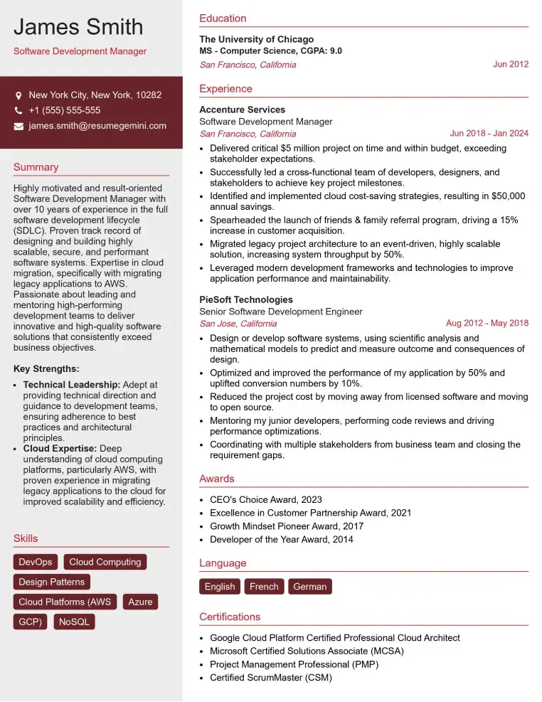
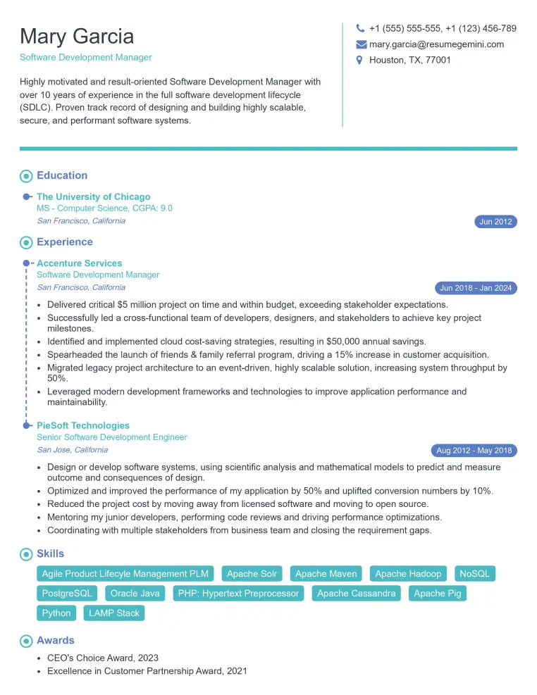
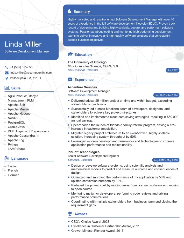
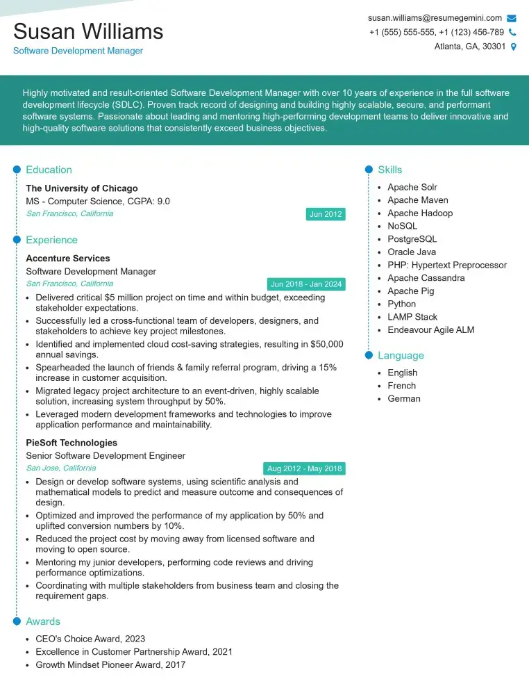
Mastering Mask Design and Development opens doors to exciting and rewarding careers in the semiconductor industry, offering opportunities for continuous learning and innovation. To maximize your job prospects, focus on building a strong, ATS-friendly resume that highlights your skills and experience effectively. ResumeGemini is a trusted resource that can help you create a professional and impactful resume tailored to the semiconductor industry. Examples of resumes specifically tailored for Mask Design and Development roles are available to guide you.
Explore more articles
Users Rating of Our Blogs
Share Your Experience
We value your feedback! Please rate our content and share your thoughts (optional).
What Readers Say About Our Blog
Hello,
We found issues with your domain’s email setup that may be sending your messages to spam or blocking them completely. InboxShield Mini shows you how to fix it in minutes — no tech skills required.
Scan your domain now for details: https://inboxshield-mini.com/
— Adam @ InboxShield Mini
Reply STOP to unsubscribe
Hi, are you owner of interviewgemini.com? What if I told you I could help you find extra time in your schedule, reconnect with leads you didn’t even realize you missed, and bring in more “I want to work with you” conversations, without increasing your ad spend or hiring a full-time employee?
All with a flexible, budget-friendly service that could easily pay for itself. Sounds good?
Would it be nice to jump on a quick 10-minute call so I can show you exactly how we make this work?
Best,
Hapei
Marketing Director
Hey, I know you’re the owner of interviewgemini.com. I’ll be quick.
Fundraising for your business is tough and time-consuming. We make it easier by guaranteeing two private investor meetings each month, for six months. No demos, no pitch events – just direct introductions to active investors matched to your startup.
If youR17;re raising, this could help you build real momentum. Want me to send more info?
Hi, I represent an SEO company that specialises in getting you AI citations and higher rankings on Google. I’d like to offer you a 100% free SEO audit for your website. Would you be interested?
Hi, I represent an SEO company that specialises in getting you AI citations and higher rankings on Google. I’d like to offer you a 100% free SEO audit for your website. Would you be interested?
good
